
Buried variation
Important defects and interfaces may not be visible from the surface.
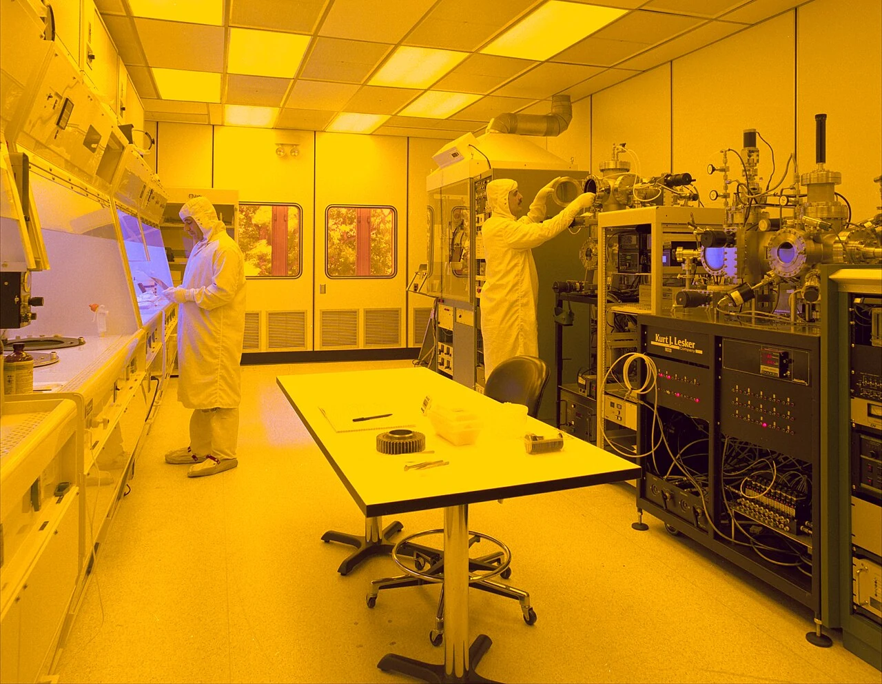
Semiconductors
As device structures, packaging, and materials become more complex, manufacturers need measurement methods that can reveal hidden physical variation without relying on destructive analysis alone.
Discuss an applicationThe operating problem
Important defects and interfaces may not be visible from the surface.
Small physical changes can create large downstream cost at production scale.
Advanced packaging introduces additional materials, interfaces, and stress fields.
A useful instrument must fit real metrology and engineering workflows.
Application pathways
Evaluate strain, field, and interface-related changes in development environments.
Support investigation of hidden changes across heterogeneous structures.
Add complementary measurement information to root-cause workflows.
Compare material and device states across controlled process conditions.
Semiconductor operating environment
 Semiconductors
 Semiconductor manufacturing
 Memory and semiconductors
 Semiconductor systems
Evaluation strategy
Every industry engagement begins with a defined target, known reference conditions, an established comparison method, and a measurable decision threshold.
Contact the applications team